Donations help to keep the site running:
Home
![]() Software
Software
![]() VHDL CPLD Course
VHDL CPLD Course
![]() Tut11 Shift Register
Tut11 Shift Register
Tutorial 11: Shift Registers in VHDL
Created on: 28 January 2013
A shift register is written in VHDL and implemented on a Xilinx CPLD. Two different ways to code a shift register in VHDL are shown.
Shift Register Operation
A register stores data i.e. logic levels, zeros and ones. A shift register has the capability of shifting the data stored in the register from left to right or right to left.
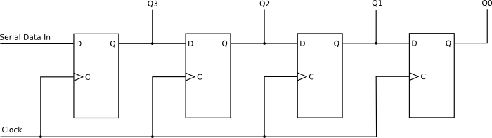
Shift registers consist of D flip-flops as shown in the figure below. This is a four bit shift register and therefore consists of four D flip-flops. This shift register is configured to shift data from the left to the right.
Data is fed into the D input of the first flip-flop on the left. This data can be either a 0 or a 1 and will be shifted to the right on each rising edge of the clock pulse. Whatever the state of the data input when the rising edge of the clock pulse occurs will be the logic level that is shifted into the first flip-flop. The data in each flip-flop will be shifted to the flip-flop on its right when the rising edge of the clock pulse occurs.
The image below shows an eight bit shift register that is created in VHDL code in this tutorial. Data is shifted from left to right – from Most Significant Bit (MSB) to Least Significant Bit (LSB).
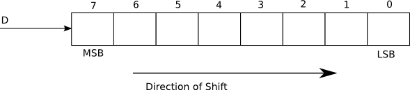
It is also possible to shift data from right to left and to use the LSB as an input for serial data.
Shift Register VHDL Code
There are two examples of a shift register written in VHDL below. The two different examples create the same shift register using slightly different VHDL code.
Both VHDL code examples of the shift register behave in exactly the same way when implemented on the CPLD.
These shift registers are both serial to parallel shift registers as they take the serial data from the D input and shift it for display on 8 LEDs in parallel.
First Shift Register
This example creates a shift register using a VHDL signal called shift_reg shown in the code listing below. This register is initialized with the value of 00h so that when power is switched on to the CPLD board, the register will be cleared. The shift_reg register is 8 bits wide and the VHDL code connects each bit in the register to an LED, so that 8 LEDs show the value in each bit of the register.
On the home built CPLD board, the LEDs will all initially be switched on because of the wiring of the LEDs to the CPLD which effectively inverts the logic level on the CPLD pin.
library IEEE;
use IEEE.STD_LOGIC_1164.ALL;
use IEEE.STD_LOGIC_UNSIGNED.ALL;

entity shift_register_top is
    Port ( CLK : in  STD_LOGIC;
           D   : in  STD_LOGIC;
           LED : out STD_LOGIC_VECTOR(7 downto 0));
end shift_register_top;

architecture Behavioral of shift_register_top is
    signal clock_div : STD_LOGIC_VECTOR(4 downto 0);
    signal shift_reg : STD_LOGIC_VECTOR(7 downto 0) := X"00";
begin

    -- clock divider
    process (CLK)
    begin
        if (CLK'event and CLK = '1') then
            clock_div <= clock_div + '1';
        end if;
    end process;

    -- shift register
    process (clock_div(4))
    begin
        if (clock_div(4)'event and clock_div(4) = '1') then
            shift_reg(7) <= D;
            shift_reg(6) <= shift_reg(7);
            shift_reg(5) <= shift_reg(6);
            shift_reg(4) <= shift_reg(5);
            shift_reg(3) <= shift_reg(4);
            shift_reg(2) <= shift_reg(3);
            shift_reg(1) <= shift_reg(2);
            shift_reg(0) <= shift_reg(1);
        end if;
    end process;

    -- hook up the shift register bits to the LEDs
    LED <= shift_reg;

end Behavioral;
Inputs and Outputs
The shift register has a D input for serial data. This input is connected to the right switch of the switch bank and feeds data into the shift register.
The CLK input of the shift register is connected to a clock source. Data is shifted in the shift register on each rising edge of the clock pulse.
The LED outputs connect each bit in the shift register to its own LED on the CPLD board.
Clock Divider
A clock divider is used to slow down the input clock so that the contents of the shift register will be visible on the LEDs.
Tutorial 6 (Clock Divider in VHDL) in this course shows how to set up the input clock for the home made CPLD board.
Doing the Shifting
The shifting inside the shift register takes place in a VHDL process. On every rising edge of the clock pulse (the divided clock pulse), the data in the shift register is shifted one bit to the right – from the MSB to the LSB.
The shifting is done by moving each bit to the bit position to its right, e.g. shift_reg(6) <= shift_reg(7); moves bit 7 to bit 6, and so on for each bit.
The source of the data being shifted is from the D input which is connected to a switch on the board. The D input is fed to the MSB of the shift register (i.e. bit 7): shift_reg(7) <= D;
Second Shift Register
The second VHDL shift register, shown below, works in exactly the same way as the first shift register except that the shifting process is simplified.
library IEEE;
use IEEE.STD_LOGIC_1164.ALL;
use IEEE.STD_LOGIC_UNSIGNED.ALL;

entity shift_register2 is
    Port ( D   : in  STD_LOGIC;
           CLK : in  STD_LOGIC;
           LED : out STD_LOGIC_VECTOR (7 downto 0));
end shift_register2;

architecture Behavioral of shift_register2 is
    signal clock_div : STD_LOGIC_VECTOR(4 downto 0);
    signal shift_reg : STD_LOGIC_VECTOR(7 downto 0) := X"00";
begin

    -- clock divider
    process (CLK)
    begin
        if (CLK'event and CLK = '1') then
            clock_div <= clock_div + '1';
        end if;
    end process;

    -- shift register
    process (clock_div(4))
    begin
        if (clock_div(4)'event and clock_div(4) = '1') then
            shift_reg(6 downto 0) <= shift_reg(7 downto 1);
            shift_reg(7) <= D;
        end if;
    end process;

    -- hook up the shift register bits to the LEDs
    LED <= shift_reg;

end Behavioral;
In the above code, the shifting is done by moving seven bits of data in a single line of code. Bits 7 to 1 (the upper seven bits) are moved to bits 6 to 0 all in one go. In other words the upper seven bits are moved right by one bit position.
New data from the D input is then fed into the MSB (bit 7).