
Understanding the 555 chip pinout is one of the first steps toward using the 555 timer IC in practical electronics circuits. The 555 is a versatile timer that can be used to generate delays, pulses, oscillations, clock signals, and switching signals. It is widely used in beginner electronics projects as well as many established circuit designs.
The 555 timer is particularly useful because its eight pins provide direct access to the internal timing and control functions of the IC. Once you understand what each pin does and how the pins work together, it becomes much easier to build, modify, and troubleshoot 555 timer circuits.
This guide explains the complete 555 chip pinout, including the function of every pin, how to identify the pins on the physical IC, how the pins interact during a timing cycle, and how the pinout is used in common 555 timer circuits.
555 Chip Pinout Overview
The standard 555 timer is an 8-pin integrated circuit. It is available in through-hole packages such as the 8-pin DIP or PDIP, as well as various surface-mount packages. The pin arrangement used by the standard 8-pin 555 timer is shown below.
When viewing a typical 8-pin 555 IC from the top, with the notch or orientation mark positioned correctly, the pins are numbered counterclockwise starting from Pin 1. On a DIP package, a notch at one end of the IC is commonly used to identify the orientation. Some packages also have a small dot or other marking indicating Pin 1.

| Pin | Name | Function |
|---|---|---|
| 1 | Ground (GND) | Connects to the negative / ground of the power supply or 0V. |
| 2 | Trigger | Starts the timing cycle when voltage falls below one-third of the supply voltage. |
| 3 | Output | Produces the high or low output signal. |
| 4 | Reset | Forces the output low when pulled low. |
| 5 | Control Voltage | Allows adjustment of internal reference voltages. |
| 6 | Threshold | Ends the timing cycle when voltage exceeds two-thirds of the supply voltage. |
| 7 | Discharge | Discharges the external timing capacitor. |
| 8 | VCC or VDD | Positive power supply. It is named VCC on bipolar 555 ICs and VDD on CMOS versions of the 555. |
The pinout is used by the classic bipolar 555 and by many compatible CMOS versions. However, identical pin assignments do not mean that all 555 devices have identical electrical characteristics. Supply voltage range, output current, power consumption, timing behavior, and other specifications can vary considerably between devices.
For this reason, always check the datasheet for the exact 555 IC being used.
555 Chip Pinout Explained Pin by Pin
Knowing the 555 chip pinout in detail helps you troubleshoot circuits and understand how the IC operates internally. Each pin function is explained below.
Pin 1: Ground or GND
Ground provides the reference point for the entire circuit. Connect this pin directly to the negative supply or circuit ground, which is sometimes called zero volts or 0V.
Pin 2: Trigger
The trigger input starts the timing cycle. When its voltage drops below approximately one-third of the supply voltage, the output switches high.
Pin 3: Output
The output pin drives external devices such as LEDs, buzzers, relays, or transistor stages. Depending on the supply voltage, it can source or sink a relatively large amount of current compared to many logic ICs. That being said, CMOS versions of the IC can usually sink and source less current than bipolar versions. Always check the datasheet for the particular 555 IC that you are using.
Pin 4: Reset
The reset pin overrides the normal operation of the timer. Pulling this pin low immediately forces the output low regardless of the other inputs.
If the reset function is not needed, connect this pin directly to the positive supply.
Pin 5: Control Voltage
This pin gives access to the internal voltage divider. Most circuits do not use it directly, but it is common practice to connect a 10nF capacitor from this pin to ground to reduce electrical noise.
Pin 6: Threshold
The threshold input monitors the timing capacitor voltage. When the voltage rises above approximately two-thirds of the supply voltage, the timing cycle ends.
Pin 7: Discharge
The discharge transistor connects this pin to ground during part of the timing cycle. It discharges the external timing capacitor and prepares the circuit for the next cycle.
Pin 8: VCC or VDD
This is the positive supply connection. Most standard NE555 devices operate from approximately 4.5 V to 16 V. CMOS versions of the 555 usually name it VDD, while bipolar versions of the 555 usually name it VCC. Some datasheets may name it differently, such as VS, or V+.
555 Chip Pinout and Internal Operation
The 555 chip pinout makes more sense once you understand how the IC works internally. Below is an image that shows the internal functional blocks of a 555 timer IC.
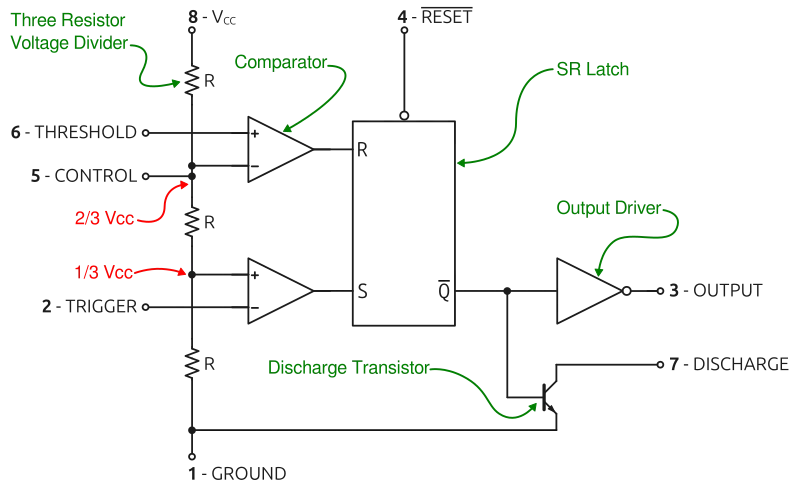
Inside the timer are:
- A voltage divider that creates one-third and two-thirds reference voltages
- Two comparators
- An SR latch
- A discharge transistor
- An output driver
The trigger and threshold pins compare the capacitor voltage against the voltage reference levels from the internal voltage divider. The latch stores the current state, while the discharge transistor controls the charging and discharging of the timing capacitor. See the 555 timer circuits article for basic configurations of the 555 IC.
This simple architecture explains why the 555 remains one of the most popular integrated circuits ever produced, as it only requires one or two timing resistors, and a timing capacitor.
NE555 Pin Configuration Compared to Other 555 Timers
The NE555 pin configuration is considered the industry standard. Modern CMOS versions, including the ICM7555, TLC555 and LMC555, use the same pin arrangement.
This means most circuits can be built using different versions without changing the PCB layout or breadboard wiring. The main differences are power consumption, operating voltage range, and output drive capability rather than the pin assignments.
Practical 555 Timer Wiring Tips
Understanding the 555 chip pinout is only part of building a reliable circuit. Correct power and component connections are also important.
Connect the Power Supply Correctly
Connect Pin 1 to ground and Pin 8 to the positive supply.
Check the required supply-voltage range for the specific 555 device before powering the circuit.
Do Not Leave Reset Floating
If reset is not being used, connect Pin 4 to the positive supply.
If reset is required for external control, use an appropriate circuit to drive it.
Consider a Control-Voltage Capacitor
A small capacitor, commonly 10 nF, can be connected from Pin 5 to ground to help reduce noise on the control-voltage input.
Follow the recommendations in the datasheet for the particular IC.
Use a Supply Bypass Capacitor
A 100 nF ceramic bypass capacitor placed close to the 555’s supply pins can help reduce supply-voltage disturbances caused by the timer switching its output.
For a breadboard circuit, placing the capacitor physically close to Pins 8 and 1 is preferable to placing it elsewhere on the breadboard.
Check the Output Load
Although the 555 output can drive useful loads, the maximum safe current depends on the particular IC.
If the circuit needs to control a relay, motor, lamp, or another relatively high-current load, use an appropriate transistor or other driver rather than assuming the 555 output can drive it directly.
Check Timing Component Values
The timing resistors and capacitor determine the timing behavior of the circuit.
Extremely high resistor values can make a circuit more sensitive to leakage currents and electrical noise. Capacitor leakage and tolerance can also become important when large-value capacitors are used.
For accurate timing, select suitable component values and consider the tolerances of both the resistors and capacitors.
Common 555 Chip Pinout Mistakes
Many problems with 555 circuits are caused by incorrect wiring rather than a defective IC.
Installing the IC Backwards
If the IC is inserted in the wrong orientation, the power connections may be applied to the wrong pins.
Always identify the package notch or Pin 1 marking before inserting the IC.
Confusing Trigger and Threshold
Pins 2 and 6 have different functions.
- Pin 2 is the trigger input and responds when its voltage falls below approximately one-third of the supply.
- Pin 6 is the threshold input and responds when its voltage rises above approximately two-thirds of the supply.
Confusing these pins can completely change the operation of a timing circuit.
Leaving Reset Floating
Pin 4 should not normally be left disconnected.
Connect it to the positive supply when reset is not being used.
Forgetting Ground
Pin 1 must be connected to the circuit ground.
A missing ground connection will prevent normal operation.
Forgetting the Power Bypass Capacitor
A 555 switches its output rapidly and can cause disturbances on the supply rails. A bypass capacitor close to the IC can help maintain a cleaner supply voltage.
Using the Wrong Supply Voltage
Not all 555 timer ICs have the same operating-voltage range.
Check the datasheet for the exact part number before applying power.
Expecting Exact Timing
The calculated timing values are theoretical. Real components have tolerances, and the 555 itself has electrical characteristics that affect timing.
For example, an electrolytic capacitor marked 100µF may have a much wider tolerance than a precision film capacitor. Leakage current can also become significant in timing circuits that use very large resistance values.
How the 555 Timer IC Pins Work Together
The 555 timer IC pins interact to create accurate timing functions.
A typical timing cycle works like this:
- The trigger pin detects a low input.
- The output switches high.
- The capacitor begins charging through a resistor.
- The threshold pin monitors the capacitor voltage.
- Once the threshold reaches two-thirds of the supply voltage, the output switches low.
- The discharge pin rapidly empties the capacitor.
- The circuit is ready for another trigger.
This sequence forms the basis of nearly every 555 timer circuit.
How to Use a 555 Timer Correctly
Learning how to use a 555 timer begins with proper wiring.
Follow these best practices:
- Double-check the IC orientation before powering the circuit.
- Connect the reset pin to VCC if it is not used.
- Add a 10 nF capacitor between the control voltage pin and ground for improved noise immunity.
- Place a 100 nF bypass capacitor close to the power supply pins.
- Use resistor and capacitor values within the recommended operating range.
- Verify the supply voltage matches the IC specifications.
These simple practices greatly improve circuit reliability.
Common Mistakes When Reading the 555 Chip Pinout
Many beginners experience problems because of a few common mistakes.
These include:
- Installing the IC backwards.
- Confusing the trigger and threshold pins.
- Leaving the reset pin floating.
- Forgetting to connect ground.
- Using incorrect resistor or capacitor values.
- Omitting supply bypass capacitors.
Most timing problems can be traced back to one of these issues.
Datasheets for the 555 Chip Pinout
There are many different manufacturers of 555 ICs and their variants. Here are links to some of their product pages where their specific datasheets are found.
Bipolar 555 IC Datasheets
| Part | Web Address |
|---|---|
| LM555 (Texas Instruments) | https://www.ti.com/product/LM555 |
| NE555 (Diodes Inc.) | https://www.diodes.com/part/view/NE555 |
| MC1455 (onsemi) | https://www.onsemi.com/products/standard-products/logic/arithmetic-logic-functions/mc1455 |
| SA555 (UMQ) | https://www.umw-ic.com/en/product_details/UMW+SA555DR |
| NE555 (UTC) | https://en.unisonic.com.tw/uploadfiles/836/part_no_pdf/NE555.pdf |
CMOS 555 IC Datasheets
| Part | Web Address |
|---|---|
| LMC555 (Texas Instruments) | https://www.ti.com/product/LMC555 |
| ICM7555 (Renesas) | https://www.renesas.com/en/products/icm7555 |
| TS555 (ST) | https://www.st.com/en/clocks-and-timers/ts555.html |
| ICM7555 (Analog Devices) | https://www.analog.com/en/products/icm7555.html |
| ALD555 / AlD7555 (Advanced Liner Devices) | https://www.aldinc.com/ald_anatimers.php |
555 Chip Pinout Frequently Asked Questions (FAQ)
What is the 555 chip pinout?
The standard 555 chip pinout has eight pins: Ground, Trigger, Output, Reset, Control Voltage, Threshold, Discharge, and VCC or VDD.
Pin 1 is Ground, Pin 2 is Trigger, Pin 3 is Output, Pin 4 is Reset, Pin 5 is Control Voltage, Pin 6 is Threshold, Pin 7 is Discharge, and Pin 8 is the positive power supply.
Is the 555 timer chip pinout the same for all manufacturers?
Yes. The 555 timer chip pinout for 8-pin ICs is standardized across most manufacturers and compatible devices, although electrical characteristics may vary slightly.
What supply voltage does a NE555 use?
A standard NE555 typically operates from about 4.5 V to 16 V. CMOS versions often support lower operating voltages.
Why is Pin 5 usually connected to a capacitor?
Pin 5 is the control voltage input. A small capacitor to ground helps filter electrical noise and improves stable operation.
Can I leave the reset pin disconnected?
No. The reset pin should normally be connected to the positive supply unless you plan to use it for external control.
Which pin provides the timer output?
Pin 3 is the output pin. It switches between high and low according to the operating mode and timing components connected to the circuit.
Which pin is ground on a 555 timer?
Pin 1 is the ground pin.
It should be connected to the negative side of the power supply or the circuit’s 0V ground connection.
Which pin is the output on a 555 timer?
Pin 3 is the output.
It provides the high and low output signal generated by the timer. The amount of current that can safely be sourced or sunk depends on the specific 555 device.
Which 555 pin is the trigger?
Pin 2 is the trigger input.
The trigger comparator responds when the voltage on Pin 2 falls below approximately one-third of the supply voltage.
Which 555 pin is the threshold?
Pin 6 is the threshold input.
The threshold comparator responds when the voltage on Pin 6 rises above approximately two-thirds of the supply voltage.
What does Pin 7 do on a 555 timer?
Pin 7 is the discharge pin.
An internal transistor can connect Pin 7 toward ground to discharge an external timing capacitor. This makes Pin 7 particularly important in astable and monostable timing circuits.
What does Pin 4 do on a 555 timer?
Pin 4 is the reset input.
Pulling Pin 4 low forces the output low and overrides normal timer operation. If reset is not required, it is normally connected to the positive supply.
What is the purpose of Pin 5 on a 555 timer?
Pin 5 is the control-voltage input. It provides access to the internal voltage reference used by the timer’s comparator circuitry.
In many conventional circuits, a small capacitor is connected from Pin 5 to ground to reduce noise.
Can I leave Pin 4 disconnected?
It is generally better not to leave the reset pin floating.
When reset is not being used, connect Pin 4 to the positive supply so that the timer remains enabled.
Is the 555 pinout the same on CMOS 555 timers?
Many CMOS 555 timers retain the standard eight-pin 555 function and pin arrangement.
However, their electrical characteristics can differ substantially from traditional bipolar 555 timers. Always check the datasheet for the exact device before substituting one type for another.
What voltage does a 555 timer need?
The required supply voltage depends on the particular 555 device.
Traditional bipolar 555 timers such as many NE555 versions generally require a higher minimum supply voltage than many CMOS versions. Some CMOS 555 timers are designed for low-voltage operation.
Check the manufacturer’s datasheet for the exact IC being used.
Do I need a capacitor on Pin 5?
A small capacitor, often around 10nF, is commonly connected between Pin 5 and ground to reduce noise on the control-voltage input.
The exact recommendation can vary by device, so the datasheet should be consulted for the particular 555 timer.
Why should I use a 100nF capacitor near the 555?
A 100nF (0.1µF) bypass capacitor placed close to the power pins helps supply transient current to the IC and reduces supply-voltage disturbances caused by switching.
It is good practice to place the capacitor physically close to the IC rather than relying on a capacitor located elsewhere in the circuit.
Can a 555 timer drive an LED?
A 555 can be used to drive an LED, provided the LED current is limited with a suitable resistor and the load is within the output specifications of the particular 555.
The LED can be connected to the output so that the 555 sources current or sinks current, depending on the circuit design.
Can a 555 timer drive a relay?
A 555 can be used to control a relay, but the relay coil should not automatically be connected directly to the 555 output.
A transistor driver and suitable protection, such as a flyback diode for a conventional DC relay coil, are commonly used to protect the timer and provide the required coil current.
555 Chip Pinout Conclusion
The 555 chip pinout is straightforward once you understand the purpose of each of its eight pins. Whether you are building a simple LED flasher, a precision delay, or an oscillator, knowing how the trigger, threshold, discharge, reset, and output pins interact is essential. Mastering the 555 chip pinout also makes it much easier to read schematics, troubleshoot circuits, and design your own timer applications with confidence.