If you’re new to electronics and want to learn how to draw a circuit diagram, this beginner guide is for you. In this step-by-step tutorial, we use KiCad, a free and powerful schematic drawing program, to create a simple 555 timer circuit that flashes a single LED. Whether you’re looking for a circuit diagram maker or exploring options for schematic drawing software, KiCad is a great place to start.
Table of Contents
- How to Draw a Circuit Diagram with KiCad
- Tips on How to Draw a Circuit Diagram
- Did You Know About How to Draw a Circuit Diagram?
- Frequently Asked Questions About How to Draw a Circuit Diagram
- Conclusion on How to Draw a Circuit Diagram
How to Draw a Circuit Diagram with KiCad
KiCad is a free and open source Electronic Design Automation (EDA) software package used to draw schematics (know as schematic capture) and for PCB design and layout. It is a CAD package for electronic circuits and is available for Linux, Windows and MacOS platforms.
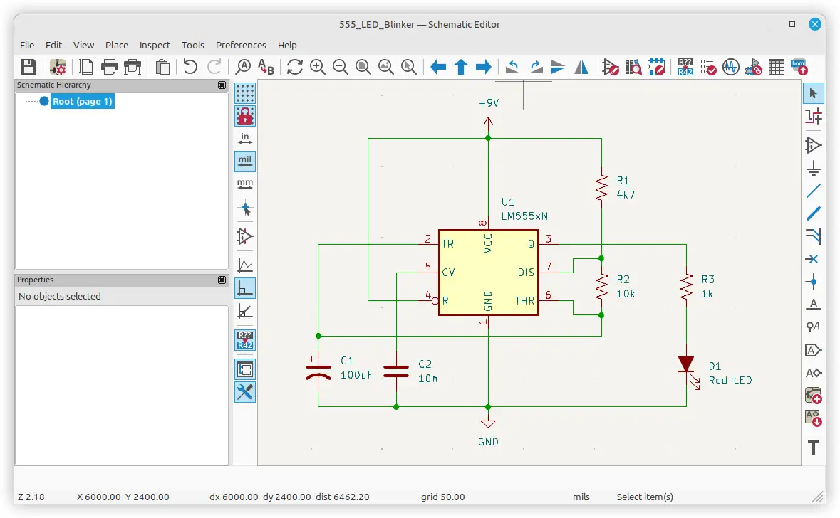
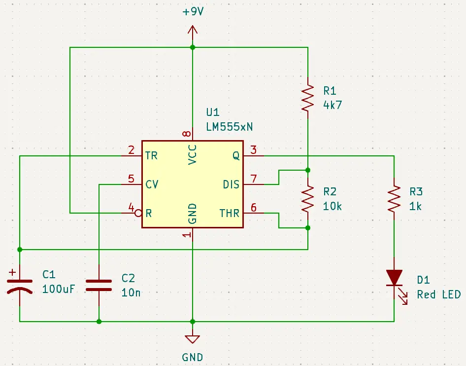
Draw a simple beginners circuit using KiCad schematic capture software and export it for displaying in documents and on the web in this tutorial. Below is the circuit diagram drawn in this tutorial. The circuit uses a 555 timer IC to flash or blink an LED.
To draw a circuit diagram using KiCad, follow these beginner-friendly steps:
1. Download and Install KiCad
You may want to check the system requirements for KiCad before starting.
Before you start, download the latest version of KiCad:
- Visit the official KiCad download page
- Choose the version for your operating system
- Follow the installation instructions
KiCad is a free, open-source electronic schematic drawing software suitable for hobbyists and professionals alike.
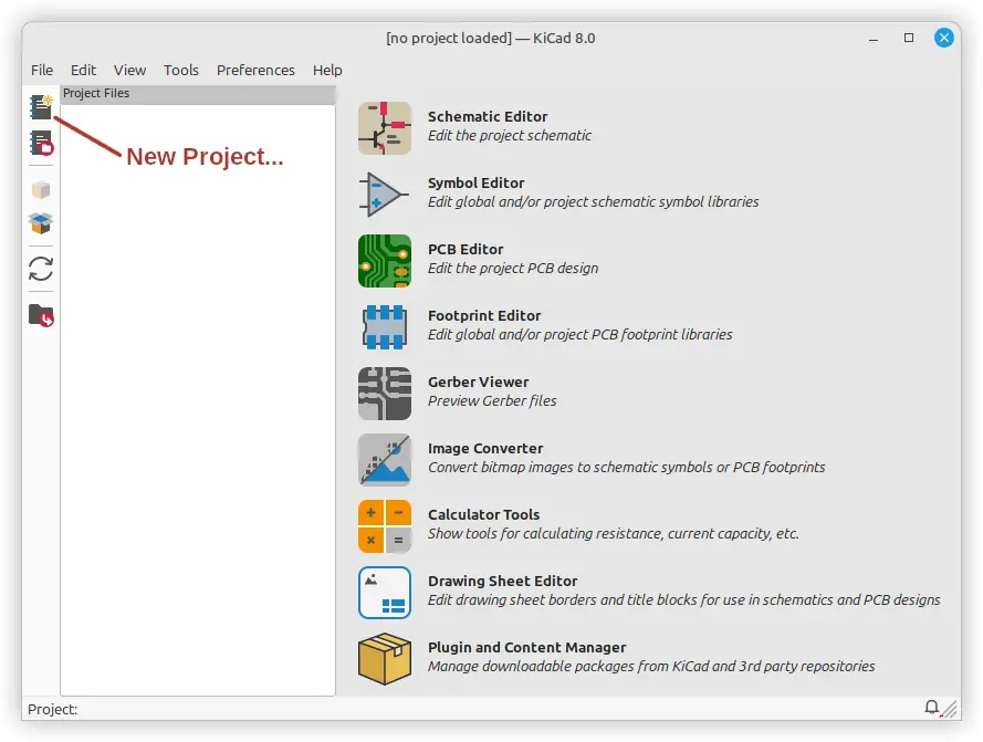
2. Launch the KiCad Project Manager
Open KiCad and create a new project:
- Click File > New Project, or click the New Project… icon, as shown in the image below
- Name your project (e.g., “555_LED_Blinker”)
- Save the project folder to your computer
You’ll see the KiCad Project Manager, which lets you access tools for schematic diagram drawing, PCB layout, and more.
3. Open the Schematic Editor
Click the Schematic Editor button to start drawing your circuit:
- This opens the schematic diagram software where you’ll place and connect components.
- This tool serves as your circuit drawer and electronic diagram maker.
4. Add Components to Your Schematic
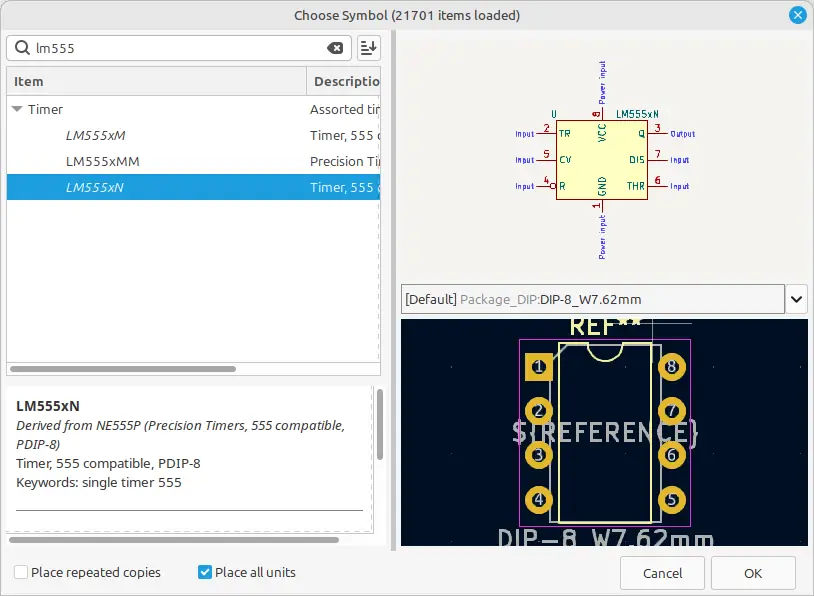
Press A on the keyboard to open the “Choose Symbol” dialog box, or select Place > Add Symbol from the top menu. In the search field of the dialog box, type the part number to find it.
For example type LM555 into the search box. To select the LM555 in a DIP package, click LM555xN in the dialog box. Finally, click the OK button in the dialog box. The following image shows the part selected in the Choose Symbol dialog box.
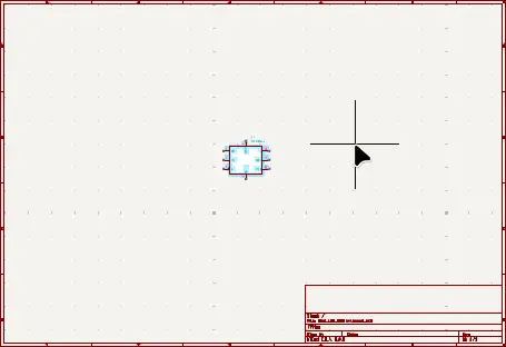
After clicking the OK button, the component is attached to the mouse cursor. Move the component to the middle of the schematic sheet and left-click the mouse button to place it. The following image shows a zoomed-out view of the schematic sheet with the component placed.
Basic KiCad Controls for Drawing and Navigation
Understanding the basic KiCad controls is essential for a smooth experience when you draw a circuit diagram. These keyboard shortcuts and mouse actions help you place components accurately, move them around, and keep your schematic organized.
Here are the essential controls every beginner should know:
Mouse and View Controls
- Mouse Wheel Scroll Up – Zoom in on the schematic at cursor
- Mouse Wheel Scroll Down – Zoom out
- Middle Mouse Button (Click + Drag) – Pan the view
- Ctrl + Mouse Wheel – Horizontal scroll (if enabled in preferences)
- Shift + Mouse Wheel – Vertical scroll (if enabled in preferences)
- F1 – Zoom in at cursor
- F2 – Zoom out at cursor
- Home – Zoom to fit page in view
- Ctrl + Home – Zoom to all objects (placed components)
Keyboard Shortcuts for Drawing
| Key | Action |
|---|---|
| A | Add component |
| P | Add power symbol (VCC, GND, etc.) |
| W | Place wire |
| N | Place a net label |
| R | Rotate selected component |
| M | Move component |
| G | Grab/move component with wires attached |
| X/Y | Flip component horizontally/vertically |
| Delete | Remove selected component or wire |
| E | Edit properties of the selected item |
| Ctrl + Z | Undo last action |
| Ctrl + Y | Redo last undone action |
Place the Components
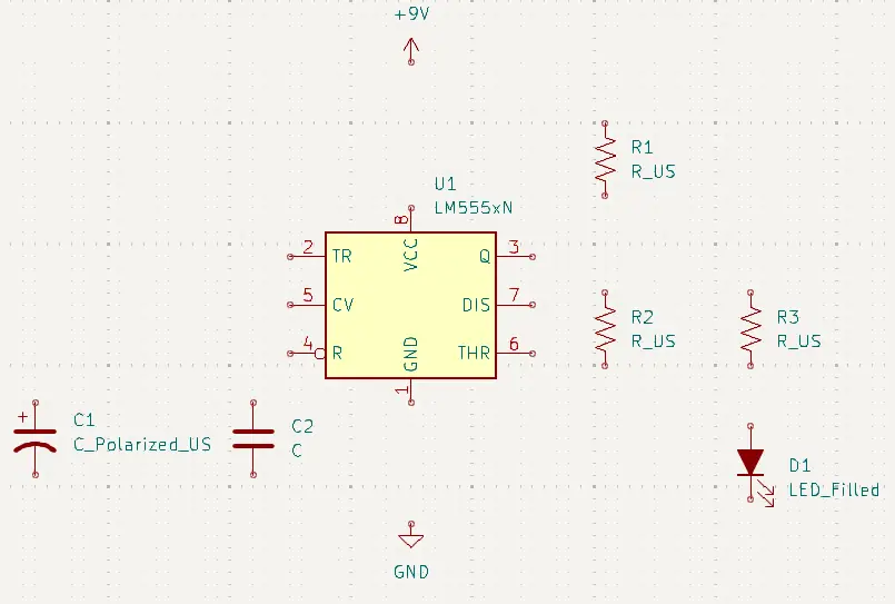
Use the parts list that follows to place the remainder of the parts in the schematic. Place the parts and then move them into approximate positions as the following image shows.
Hover the mouse cursor over the body of a part and press the M keyboard key to select the part for moving. Be careful not to select the text of the part that is outside the part body, as this will then be moved instead of the part. Press the keyboard Esc key to stop moving the part or text if accidentally selected. Move the part with the mouse cursor and click the left mouse button to place the part.
With a part selected for moving, press the R key to rotate it 90 degrees at a time. This also works when hovering the mouse cursor over a part that is not selected for moving.
Parts to Place
Search for and add these components:
- NE555 or LM555 (555 Timer IC): search for NE555P or LM555xN
- Resistors (3x): search for R or R_US – after placing one resistor, press the keyboard Insert key to insert subsequent resistors
- Polarized capacitor (1x): C_Polarized or C_Polarized_US
- Non-polarized capacitor (1x): C
- LED (1x): LED or LED_Filled
- Power symbols (VCC and GND): +9V and GND
Your parts list for this simple LED flasher:
| Designator | Component | Value | KiCad Part |
|---|---|---|---|
| U1 | 555 Timer IC | NE555 or LM555 | NE555P or LM555xN |
| R1 | Resistor R1 | 4k7 | R for EU symbol, or R_US for US symbol |
| R2 | Resistor R2 | 10k | R or R_US |
| R3 | Resistor R3 | 1k | R or R_US |
| C1 | Capacitor C1 | 100 µF | C_Polarized for EU symbol, or C_Polarized_US for US symbol |
| C2 | Capacitor C2 | 10n | C |
| D1 | LED | Red LED | LED or LED_Filled, depending on your preference |
| +9V | Power Supply | 9V Battery + terminal | +9V |
| GND | Power Supply | 9V Battery – terminal | GND |
5. Change the Component Values
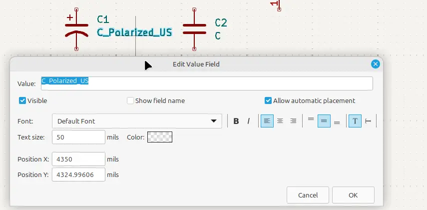
Hover the mouse cursor over the value text of each component and then press the E key to edit this text. Give each component the correct value as shown in the previous table. For example, hover the mouse cursor over the C_Polarized_US or C_Polarized text of C1 and press the E key. In the dialog box that pops up, type in 100uF for its value, as the following image shows.
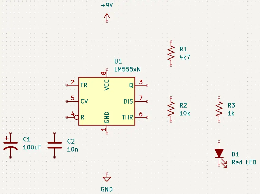
After changing the component values, your circuit diagram should look similar to the following image.
6. Wire the Circuit
Use the Place Wire (W) tool to connect components. That is, place the mouse cursor over the end of the pin to connect and then press the W keyboard key. The basic wiring for this 555 timer circuit is:
- Pin 1 (GND) to ground
- Pin 8 (VCC) to positive voltage (+9V)
- Pins 4 and 8 connected together (reset to VCC)
- Capacitor C1 between Pin 2 and GND
- Capacitor C2 between Pin 5 and GND
- R2 connects Pin 7 to Pin 6
- Connect Pin 6 to Pin 2
- R1 connects Pin 7 to VCC (+9V)
- LED and current-limiting resistor (R3) connected to output pin (Pin 3) and GND
How to Wire Components in KiCad
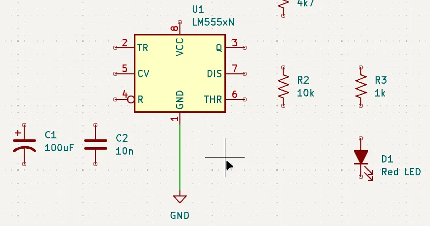
To complete the first wiring step in the previous list, hover the mouse cursor over pin 1 of the 555 timer, U1. Next, press the W key on the keyboard. This connects a wire to pin 1. Now move the mouse cursor down and hover it over the pin of the GND component. A green wire should extend down when moving the cursor. Either press the W key again or click the left mouse button to wire the IC pin to the GND.
If a wire is bending at 90 degrees in the wrong direction, press the forward slash keyboard key / to make it change direction. This key is near the bottom right of the keyboard, to the left of the right Shift key on US keyboards. It is the question mark ? and forward slash key /.
To join a wire to a wire, simply move the cursor to the part of the wire to connect to and click. Of course this is when the wire is already connected to a pin at the other end. A small junction dot or node is automatically inserted where the wires join.
The following image shows pin 1 of the 555 timer IC connected to GND with a wire.
Continue wiring the components in the circuit diagram until they are all connected as the following image shows. Move the components as needed to make the wiring line up. Drag a component by hovering the cursor over the component and pressing the G key. As a result, the component can be moved with the wiring still attached to it.
7. Electrical Rules Check (ERC)
Run an ERC to verify that your circuit is correctly wired:
- Click Inspect > Electrical Rules Checker
- In the dialog box that opens, click the Run ERC button
- Fix any warnings or errors shown
In this circuit you will probably get the following error message twice:
Error: Input Power pin not driven by any Output Power pins
To correct this error, simply place two PWR_FLAG components on the schematic. Connect one to the positive wire that connects to VCC / Pin 8 of the 555 and to +9V. Connect the second PWR_FLAG to the GND wire.
8. Exporting the Circuit Diagram for Documents and Web
Circuits can be exported into different formats for displaying in documents and on the web. For example SVG format can be used in documents and on the web. KiCad circuits can also be exported to PDF and several other formats.
To export a circuit, use the Plot facility. On the top menu bar, select File > Plot. In the dialog box that pops up, the Output directory field can be left blank. Leaving this field blank will save the exported file to the current project’s folder.
Uncheck Plot drawing sheet to export the circuit from the schematic page without the border and title block, if desired. In the Output Format box, select the desired export format. SVG will work in web pages and should work in documents as well. PDF can be selected to export the circuit diagram to a PDF file.
When finished selecting the plot setting, click the Plot Current Page button. You will find the exported file in the project folder.
If further editing of a SVG file is needed, it can be edited in a program such as Inkscape.
Tips on How to Draw a Circuit Diagram
Here are practical tips to help you get started with any schematic diagram program:
- Label your nets clearly: Use meaningful net names like “LED_OUT” or “TIMER_OUT”.
- Keep spacing clean: Leave space between components to avoid overlapping wires.
- Use power symbols instead of drawing long wires for VCC and GND.
- Group related components (e.g., timing parts near the timer IC).
- Use ERC often to catch common wiring mistakes early.
These habits will improve your schematics and make the transition to PCB design smoother.
Did You Know About How to Draw a Circuit Diagram?
- The earliest schematic diagrams were hand-drawn, often with ink and rulers.
- KiCad originated in the 1990s and has since become a widely-used software to make schematic diagrams in both academia and industry.
- The 555 timer IC, invented in 1972, is one of the most popular ICs ever made—perfect for beginner projects in any schematic diagram drawing software.
Frequently Asked Questions About How to Draw a Circuit Diagram
What is the best free circuit diagram creator?
KiCad is one of the best free circuit diagram makers. It offers full schematic capture and PCB layout functionality.
Is KiCad good for beginners?
Yes. KiCad is beginner-friendly with many tutorials available, and it supports everything from simple circuits to complex PCB design.
Can I simulate the circuit in KiCad?
Yes, KiCad includes simulation capabilities using the ngspice engine, though beginners may prefer to focus on drawing the circuit first.
What is the difference between schematic and wiring diagram?
A schematic diagram shows logical connections and symbols, while a wiring diagram shows actual physical layout and wire colors.
What other tools can I use to draw a circuit diagram?
Besides KiCad, other options include EasyEDA, Fritzing, and LTspice. However, KiCad stands out as a robust schematic diagram drawing software.
Can I export my KiCad schematic?
Yes, KiCad allows export to PDF, SVG, and other image formats for sharing or printing your electronic schematic drawing.
Conclusion on How to Draw a Circuit Diagram
Learning how to draw a circuit diagram using KiCad is a valuable skill for anyone entering the world of electronics. This beginner tutorial walked you through installing KiCad, using it as a circuit diagram creator, and building a classic 555 timer LED flasher. With practice, you’ll be able to use KiCad and other schematic drawing software to design more advanced circuits confidently.
Whether you’re a student, hobbyist, or aspiring engineer, starting with the right schematic diagram program makes all the difference.
For another example of a circuit drawn using KiCad, see the LED flasher circuit project.